Pre-Shipment PCB Inspection Checklist for B2B Buyers
Verify board quality before accepting delivery by checking solder joints, component placement, and visual defects. This pre-shipment check uses standard acceptance criteria to identify faults early, reducing rework, warranty claims, and production downtime for B2B buyers.
- A structured PCB inspection checklist catches solder defects, component errors, and contamination before the board leaves the factory.
- Define acceptance criteria with your supplier so both teams use the same standard for "pass" and "fail."
- Check both visual defects and hidden defects such as buried solder joints and component orientation.
- Use the checklist to verify documentation, handling, and packaging alongside the physical board.
- Keep records of inspection findings to support claims and improve future production runs.
Start with the Right Documentation Before You Open the Box
Do not inspect a board until you confirm the paperwork matches the order. Pull the purchase order, the engineering drawing revision, the bill of materials, and the certificate of conformity. Verify that the revision number on the board silkscreen matches the approved drawing. A mismatch here means the board may have the wrong component values, the wrong footprint, or the wrong netlist. It also changes your acceptance criteria because the spec you are testing against is no longer the one you approved.
Check the certificate of conformity for the lot number, the date of manufacture, and the test method used. If the supplier only provides a generic “passed inspection” note without the test method, request the detailed report. The test method matters. A board that passed a visual check is not the same as a board that passed a full AOI run with a 0.5 percent defect tolerance.
Visual Inspection: Surface Mount and Through-Hole Components
Begin with the top side of the board. Use a magnifying lamp or a basic stereo microscope if you do not have one on hand. A 5x to 10x magnification is enough for most surface mount checks. Look for lifted leads, missing components, and components that are not seated flat.
Check the orientation of each component. A resistor that is installed upside down may look fine from the side, but the polarity marker will be wrong. A diode with the cathode stripe facing the wrong way will fail immediately. A capacitor that is placed vertically instead of horizontally will not solder properly and will crack under vibration.
For through-hole components, check the lead placement. The lead should go through the hole and be bent away from the board surface. A lead that sits flat against the board surface indicates a bad solder joint. It will not make a reliable electrical connection. It will also create a stress point that can crack the solder over time.
Solder Joint Quality: The Core of PCB Inspection
Solder joint quality is the most common failure point in printed circuit board assembly. Inspect every visible joint. A good solder joint has a smooth, concave fillet that forms a clean curve where the lead meets the pad. The fillet should be uniform in height and width.
Look for these defects:
- Cold solder joints. The joint looks dull, grainy, or broken. This happens when the solder did not reach the correct temperature. The joint will have a weak bond and can crack under vibration or thermal cycling.
- Solder bridges. Excess solder connects two adjacent pads. This creates a short circuit. It is easy to see with the naked eye but can be missed if the pads are closely spaced.
- Solder balls. Small spheres of molten solder sit on the board. They can roll off during handling or create shorts if they land on a live pad.
- Tombstoning. A surface mount component stands up on one end. This usually happens when the solder paste is unbalanced or the component is not placed correctly.
- Missing solder. The joint looks bare or the lead does not touch the pad. This is a non-functional joint.
For buried solder joints, such as those under a QFN or BGA package, a visual check is not enough. These joints are hidden under the component. You need X-ray inspection to verify them. If your acceptance criteria require buried joint verification, confirm that the supplier used X-ray and provide the report. A visual check of the component edge does not tell you the internal state of the solder.
Component Placement and Orientation
Check every component against the assembly drawing. Verify the part number, the value, and the orientation. A 10k resistor placed where a 1k resistor belongs will pass a visual check but fail in the field. A 100nF capacitor placed where a 1000nF capacitor belongs will change the circuit behavior in a way that is not visible from the board surface.
Check the polarity of every diode, transistor, IC, and electrolytic capacitor. The cathode stripe on a diode must match the pad marking on the board. The negative terminal of an electrolytic capacitor must match the marked pad. The pin 1 dot on an IC must align with the silkscreen dot.
For surface mount components with a single-sided orientation, check the marking. A component with a “1” on one corner must have that corner aligned with the silkscreen “1.” A misaligned component will not function correctly even if the solder joint looks perfect.
Contamination and Board Surface Check
Inspect the board surface for flux residue, solder splatter, and foreign material. Flux residue is not always a problem, but it can attract moisture and cause corrosion over time. If your acceptance criteria require clean boards, verify that the flux has been removed and the board is dry.
Check for solder splatter on the dielectric surface. Solder that has splashed onto the board surface can create a short circuit. It is especially dangerous on high-speed boards where the impedance is tightly controlled. A small glob of solder on a trace can change the impedance and cause signal reflections.
Look for scratches on the copper traces. A scratch that reaches the copper can create a partial short or a high-resistance connection. It is hard to see with the naked eye. A high-magnification inspection or an electrical test is required to catch these.
Electrical and Functional Verification
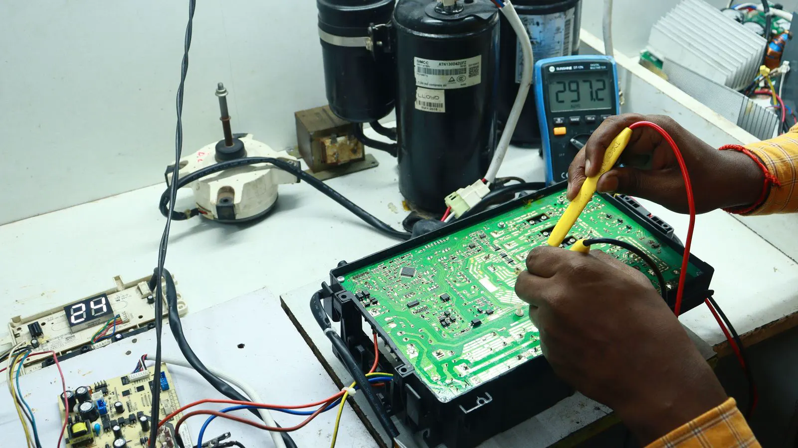
Visual inspection is not enough. A board can look perfect and still fail electrically. Run an open-short test to verify that no traces are shorted and no traces are open. This test is fast and catches most solder bridge defects that a visual check missed.
If your acceptance criteria include functional testing, run a simple power-on test. Verify that the board powers up without protection tripping. Check the main voltage rails with a multimeter. If the board has a microcontroller, verify that it boots to the expected state. If the board has a display, verify that it lights up.
For boards with high-speed signals, verify the impedance with a TDR if available. A solder joint that looks fine can still have a high resistance that causes signal degradation. A TDR test will catch these issues before the board goes into production.
Packaging and Handling Verification
Before you accept the board, check the packaging. The board should be in anti-static packaging. If the board is in a standard cardboard box without anti-static protection, it may have been exposed to electrostatic discharge. This can damage sensitive ICs even if the board looks fine.
Check the board for physical damage. Look for bent pins, cracked components, and warped boards. A warped board is a sign of poor manufacturing or thermal stress. It will not seat properly in a connector and can crack during assembly.
Verify the quantity. Count the boards against the packing list. A missing board is a supply chain issue that will delay production. It is easier to catch now than after the board has been installed in a product.
Acceptance Criteria: What Passes and What Fails
The most common mistake is to have no written acceptance criteria. “Looks good” is not a standard. Define what you accept and what you reject. Write it down. Share it with your supplier. Use it for every inspection.
Use a table to define your acceptance criteria for each defect type. This makes the inspection process repeatable and reduces disputes.
| Defect Type | Acceptance Criteria | Action |
|---|---|---|
| Solder bridge | No visible solder connecting two pads | Reject lot, request rework |
| Cold solder joint | Dull, grainy, or broken fillet | Reject board, request rework |
| Component missing | Any required component absent | Reject board, request rework |
| Flux residue | Visible residue on dielectric surface | Clean or reject based on spec |
| Solder ball | Any ball on a live pad | Reject board, request rework |
| Buried joint | No X-ray report provided | Request X-ray report before acceptance |
If a defect falls outside your acceptance criteria, do not accept the board. Return it to the supplier with a clear description of the defect. Include photos and the lot number. This creates a paper trail that supports your claim and helps the supplier improve the process.
Record Keeping and Continuous Improvement
Keep a log of every inspection. Record the date, the lot number, the number of defects found, and the action taken. This data will show you which defects are most common. It will also show you whether a specific supplier or process is causing more failures than others.
Share this data with your supplier. A supplier that receives regular feedback on defects will improve their process. A supplier that does not receive feedback will repeat the same mistakes. The data is the most valuable tool you have for improving board quality over time.
Use the checklist above for every shipment. Do not skip steps because the board looks good. A board that looks good can still fail. The checklist is your defense against hidden defects, documentation errors, and supply chain mistakes.
Frequently asked questions
What is the minimum inspection level for B2B PCB shipments?
Verify the documentation, check the visual solder joints, confirm component placement, and run an open-short test. These four steps catch most common defects before acceptance.
How do I handle a board with minor defects that do not affect function?
Define your acceptance criteria in writing before the first shipment. If a defect is outside the criteria, reject it. If it is inside the criteria, accept it and record it for future reference.
Do I need X-ray inspection for every board?
No. X-ray is required only for buried joints such as BGA and QFN packages. For simple surface mount and through-hole boards, a visual and electrical check is usually sufficient.
What is the fastest way to catch a solder bridge?
Run an open-short test. A visual check can miss small bridges between closely spaced pads. An electrical test will detect them immediately.
How do I dispute a defective board with the supplier?
Use the acceptance criteria you agreed to in writing. Provide photos, the lot number, and the specific defect. Reference the checklist item that was violated. This makes the claim clear and actionable.